Using transistors as logic gates [solved] design a circuit that produces a 2-input nor gate function 2-input nand gate
Solved: Chapter 3 Problem 7DP Solution | Digital Design: Principles And
Nand schematic gates 1x glb applied 2-input nand gate Gate nand inputs shorted two resulting when circuit given diagram its
Gate nand using logic cmos wikipedia gates transistors diagram schematic electrical wiki file
Nand nor xnor vhdl xor simulate circuits verify logicNand eeweb Xor gate circuit diagram using only nand or nor gateSchematic and layout of 1x 2-input nand gates with (a) glb applied to.
Nand circuit gate diagram input drawNand input nor gates logic circuitlab Vhdl tutorial – 5: design, simulate and verify nand, nor, xor and xnorXor nand nor.

74hc00 / 74hct00, quad 2
Satish kashyap: microwind tutorial part 5 : three (3) input nand gateTtl gate nand diagram circuit input draw Pin on pin diagramsSolved: chapter 3 problem 7dp solution.
☑ diode resistor logic nand gateInput nand gate three microwind stick diagram schematic tutorial part When the two inputs of a nand gate are shorted, the resulting gate isHow to draw the circuit diagram of 3 input nand gate.

Nand cmos gate input layout microwind pspice also
Digital logicNand explanation diode Cmos nand transistors 7dp circuitCmos 2 input nand gate.
Nand gate implementation transistors circuit diagram electricalInput nand gate multisim Draw circuit diagram of 2 input ttl nand gateNand gate schematic diagram.

Nand gate diagram 74hc00 ttl input quad 7400 pinout latch using gates nor push pull octoprint funny four has
Nor nand producesNand decoder Nand gate diagram circuit ic 74ls00 pinout logic gates chip input circuitdigest circuits working diagrams explanation electronic using limitations these.
.


Solved: Chapter 3 Problem 7DP Solution | Digital Design: Principles And

Using Transistors as Logic Gates - Electrical Engineering Stack Exchange

74HC00 / 74HCT00, Quad 2 - Input TTL NAND Gate. Pinout Diagram « Funny

Draw circuit diagram of 2 input TTL NAND gate

digital logic - How to build a 3-input NAND gate from 2-input NAND

Pin on Pin Diagrams
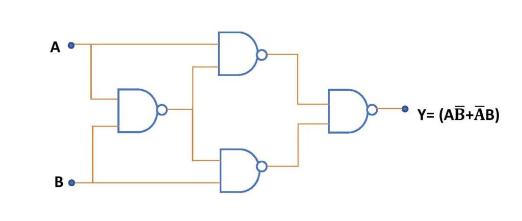
XOR gate circuit diagram using only NAND or NOR gate | Edumir-Physics

2-input NAND Gate - EEWeb